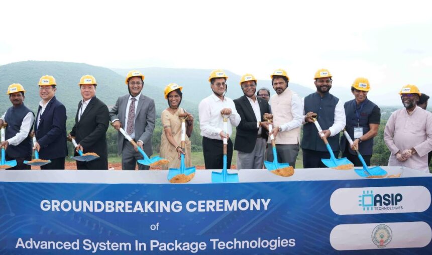
August 3, 2026, Vishakhapatnam: ASIP Technologies has begun work on a ₹2,500-crore advanced semiconductor packaging facility in Andhra Pradesh, marking South India’s first Outsourced Semiconductor Assembly and Test (OSAT) project approved under the India Semiconductor Mission (ISM 1.0). The investment positions the state among India’s emerging semiconductor manufacturing destinations while strengthening the country’s capabilities in advanced chip packaging, a critical yet underdeveloped segment of the semiconductor value chain.
Prime Minister Narendra Modi virtually laid the foundation stone for the project at Tarluvada, Visakhapatnam, with Andhra Pradesh Chief Minister N. Chandrababu Naidu joining the ceremony remotely.
Addressing the event, the Prime Minister said Andhra Pradesh is looking to the future by investing in sectors such as semiconductors, information technology and innovation, adding that the state’s growing focus on advanced manufacturing will create new opportunities for its youth. He also noted that Andhra Pradesh, known for its software talent, is now well positioned to emerge as a semiconductor manufacturing hub with continued support from the Centre under the Viksit Bharat mission.
The 30-acre facility will be developed with an initial investment of over ₹460 crore in partnership with South Korea-based APACT Co., which will provide advanced packaging technology. ASIP plans to invest an additional ₹2,000 crore in subsequent phases, taking the total project investment to ₹2,500 crore.
Once operational, the plant will have the capacity to package and test up to 96 million semiconductor units annually, serving applications across artificial intelligence (AI), high-performance computing (HPC), data centres and high-speed communications.
The ASIP facility will initially support wire-bond and Flip-Chip Ball Grid Array (FC-BGA) packaging before expanding into 2.5D and 3D advanced packaging technologies within the next two to three years. These technologies are increasingly becoming central to next-generation AI processors and high-performance computing chips, where packaging innovation is driving performance improvements alongside advances in silicon.
Unlike wafer fabrication, which demands significantly higher capital investment, OSAT facilities offer countries a faster entry into semiconductor manufacturing while addressing a strategic gap in the global supply chain. Packaging and testing account for nearly 30% to 40% of a semiconductor’s manufacturing value, yet India continues to rely heavily on overseas facilities for these critical processes.
Speaking at the event, Amitesh Kumar Sinha, Chief Executive Officer of the India Semiconductor Mission, described the project as an important addition to India’s semiconductor programme, saying advanced packaging capacity will play a key role in strengthening the country’s electronics manufacturing ecosystem.
South India’s First OSAT Plant by ASIP Signals India’s Next Semiconductor Manufacturing Milestone
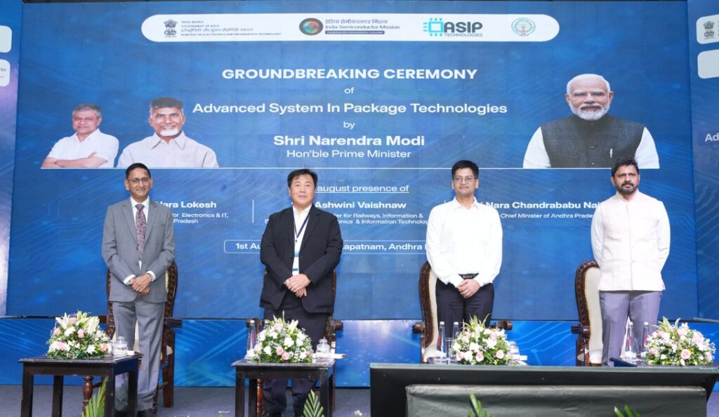
ASIP Managing Director and Chief Executive Officer Venkata Simhadri said the company aims to establish world-class semiconductor assembly, packaging and testing capabilities while accelerating supply-chain localisation and workforce development in India.
APACT President and Chief Executive Officer Seong Dong Lee said the partnership combines South Korea’s packaging expertise with India’s engineering talent at a time when semiconductor companies are diversifying manufacturing locations and building more resilient global supply chains.
The project is expected to create more than 1,000 direct high-skilled jobs and 1,600 indirect jobs. ASIP also plans to establish an in-house semiconductor training centre and collaborate with institutions including IIT Tirupati and IIT Hyderabad to build a skilled talent pipeline for India’s growing chip industry.
The facility will integrate sustainability measures, including solar power generation and water recycling systems, as part of its manufacturing operations.
For India’s semiconductor ambitions, the Visakhapatnam project represents more than another manufacturing investment. As artificial intelligence, advanced computing and heterogeneous chip architectures reshape the semiconductor industry, advanced packaging has emerged as one of the fastest-growing segments of the value chain.
By establishing domestic OSAT capabilities, ASIP is positioning India to capture a larger share of semiconductor manufacturing beyond chip design, while reducing dependence on overseas packaging and testing facilities.